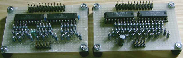
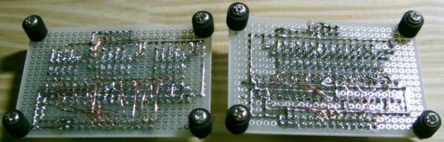
Prototype 1
My first FPGA project started off as a PCE hardware preservation project. But since it was too difficult for me to start from there, I down-sized the project to the FC, which is known as the model hardware of the PCE. I will go back to the PCE project after this project is more or less complete. I'm not the first one, but probably 4th or 5th, to implement the FC on the FPGA (on the net), but that doesn't really matter because I wanted to make my own anyway.
I don't plan to open the IP to the public at the moment.
| Mario Bros. | 99% | |
|---|---|---|
| Super Mario Bros. | 99% | |
| Wrecking Crew | 99% |
| Star Soldier | 99% | |
|---|---|---|
| Hector 87 | 95% |
| DQ1 | 99% | |
|---|---|---|
| DQ2 | 99% | |
| DQ3 | 0% | |
| DQ4 | 0% |
| FF1 | 99% | |
|---|---|---|
| FF2 | 99% | |
| FF3 | 80% |
The image at the top of this page probably gives you an idea of how it works.
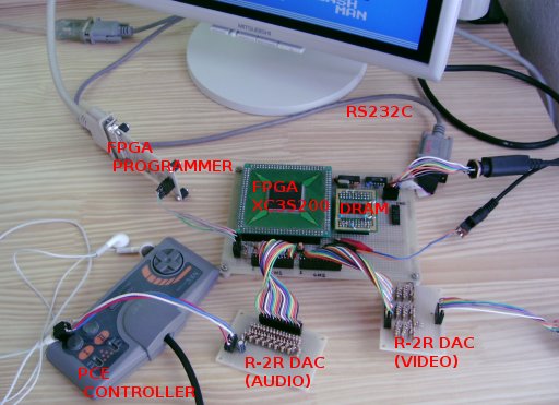
The clock is 21.47727[MHz]. Using this frequency will display about 540 horizontal pixels on VGA monitors. Since FC's horizontal resolution is 256, I will stretch it by 2 times, and I think there will be some black areas on the left & right sides.
The DRAM MT4LC4M16R6 is 4Mx16-bit EDO-DRAM, although I don't plan to use the EDO mode. ROM images are downloaded into the DRAM prior to running. Since it is a DRAM, it requires data refreshing, and basically you can't access data during the refresh cycles. But in the case of FC the CPU only runs at 1/12 (=1.789772[MHz]) of the master clock frequency, and the refresh can easily be done in the remaining 11/12 clock cycles.
Although you can't see it in the photo, there is a 32kB SRAM mounted under the FPGA. This SRAM will be used for character ROM/RAM.
I used a PCE controller. Since it has a turbo feature, you can play games as if you play it with the Joy Card mkII.
R-2R DAC is used for audio and video outputs at the moment. R=150[Ohm] is used. There is no reason for using 150-Ohm resistors, but these work pretty well with my iPod earphone and LCD diplay. (^_^;
The squence of downloading program to prototype 1 board at the moment:
The CPU is written totally from scratch, reflecting what I experienced with the PCE CPU core. It is implemented so that the number of cycles to execute instructions are the same as the real 6502. I wrote an instruction decoder rather than writing microcode (ROM) this time. Although it was just too buggy at the beginning, some games started to work after constantly fixing the bugs.
The CPU uses 400+ slices, which seems small enough.
I compared result of the Icarus Verilog simulator with result of a 6502 emulator I made in the past to test my 6502 core. I wrote a program to generate a test ROM image containing randomly generated opcode and operands which also takes care of CPU not to jump into invalid addresses, access invalid locations, etc. Undocumented instructions are defined in the enum table, but these instructions are not generated at the moment.
One of differences between my 6502 and the real one is that
my 6502 has separate "/RD" and "/WR" signals while the real 6502 has "R/W" only
(which means all cycles other than write cycles are read cycles).
This is to prevent my 6502 from accidentally reading from addresses such as
$2002 and $4015 on cycles where it only updates lower or upper byte of the address
by holding both "/RD" and "/WR" to high.
Sep.19 2008: I later noticed that the real FC/NES 6502 is known to read from
address with only lower byte updated. For example, STA $700,X does a dummy
read from $0700 before it finally writes to $(0700+X). Furthermore,
instructions which do addition to effective addresses and generate carry to
high address bytes such as STA $20F2,X (X=$10) does a dummy read from
$2002(!) and then write value of A to $2102. So the conclusion here is that
separating the "R/W" signal to "/RD" and "/WR" was totally unnecessary. :-(
Another difference is that my 6502 does everything in synch with positive edge of the clock signal. The real FC/NES 6502 updates address and control signals at negative edge of Phi2, and output data at the following positive edge. This is because using both edges of the clock on FPGA vastly decreases maximum operating clock frequency.
One major disadvantage of not using both edges of the clock signal is that you can't update internal state on every clock cycle when you use synchronized devices such as Block RAM, because such devices need one clock cycle to reflect the input to the output. Although this is also true for my 6502, this is not a problem this time since my 6502 operates at 1.79[MHz] and the master clock is 12 times the frequency (21.48[MHz]), and so there are 11 positive edges between a state update to another.
Some other major differences are that my 6502 does not support undocumented instructions, and RMW instructions does not operate as RMWW (it is know that FC/NES 6502 writes a garbage data to effective address before it finally writes the correct one). So I have to say that the compatibility of my 6502 is rather poor. But at the same time there are only few programs which rely on these characteristics.
The horrifying thing would occur if a program executes a RMW instruction to a "double-write register". In the case of FC/NES, registers $2005 and $2006 are double-write registers. For example, if INC $2005 is executed, the results of my 6502 and the real one are different. While my 6502 does not complete the double write, the real FC/NES 6502 does. So the rest of the executed code on my 6502 can give completely incorrect result.
[UNNECESSARY NOTE] Although I haven't seen any code which execute RMW towards FC/NES registers,
I have seen a code which resets the MMC1 chip by an INC instruction. It actually
reads a ROM location containing a value of $80, increments the value, and writes
the result to the MMC1. My assumption is that the first write to the MMC1 is the
value before increment, so it's probably $80. Then it writes $81 to the MMC1.
If this is the case, then it's a transition of the D0 bit from 0 to 1 while holding
the D7 bit 1. I don't know how the MMC1 exactly behaves with this sequence, but it
must be either the MMC1 being reset twice or the MMC1 not reset on the $80 write,
and then reset by the $81 write (not verified). Although the FC/NES 6502 is not
completely same as the general NMOS6502 chip, it has been verified that the FC/NES 6502
also has undocumented instructions and executes RMWW for RMW instructions.
[Aug.02 2008]
Fixed a bug in the LDY $ABS,X instruction. The /RD signal was not asserted. The RAM simulator I wrote was so sloppy that it was possible to read out its data without asserting the /RD. That made it impossible to find this bug on the simulator, and I was forced to debug the instruction on the FPGA. :-(
Although not very accurate, I partially implemented the APU. It uses R-2R DAC for the audio output. The DAC is 16 bits in resolution, but it probably won't give the full 16 bit precision since all resistors are with 5% error at maximum. Actually only the upper 10 bits are used. Music is played after downloading and running a game program.
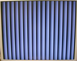
I implemented a gradated grayscale color bars to see the precision of my R-2R DAC. Although you can't really see it in the photo, some vertical lines of strange colors are noticeable. This is probably due to the error of resistors in the R-2R DAC (resistors with 5% tolerance are used). But I assume it's good enough for a prototype.
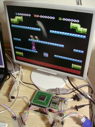
Implemented the backgound processing. Vertical scroll works pretty well, but horizontal scroll is rough since it's still tile based. I had been worring about the aspect ratio since the display is VGA, but it turned out to be pretty good. Sprite is not implemented yet.
The FC's screen resolution is 256x240, and it doesn't match the VGA timing. Also the 256x240 is too small for the VGA screen. So the image is internally "up-scan converted" to double both horizontally and vertically.
Implemented horizontal scrolling. Although I don't know exactly how the real hardware implements this feature, it must be using shift registers to shift data read from pattern table, and finally getting pixels as output. The assumption is probably correct since this is probably the simplest way of taking out bit data as a pixel, and also according to Brad Taylor's document.
According to Brad Taylor's document "2C02 technical reference.txt":
For determining the precise delay between when a
tile's bitmap fetch phase starts (the whole 4 memory fetches), and when the
first pixel of that tile's bitmap data hits the video out pin, the formula
is (16-n) clock cycles, where n is the fine horizontal scroll offset (0..7
pixels).
If we take the (16-n) into account, it is probably natural to think that there is a 16-bit shift register with the lower 8 bits capable of loading data. Why is the delay affected by the fine horizontal scroll offset? This is probably because the bit position fetched as pixel output is selected by the fine horizontal scroll offset.
 |<-- Select by H-SCROLL[2:0] -->|<------- Load & Shift -------->|
 +---+---+---+---+---+---+---+---+---+---+---+---+---+---+---+---+
 |   |   |   |   |   |   |   |   | 7 | 6 | 5 | 4 | 3 | 2 | 1 | 0 |
 +---+---+---+---+---+---+---+---+---+---+---+---+---+---+---+---+
                    <-- Shift Direction (shift on every dot cycle)
The pixel data fetched is the very last bit of the shift register when
the fine horizontal scroll offset is zero, it's one bit next to the
last one when the horizontal scroll offset is 1, ... Horizontal
scroll feature within a tile can be done this way. And horizontal
scrolling of the whole screen can be done by applying this method
to all tiles drawn on a scanline.
With the above structure, it takes only 8 cycles between when data is loaded into the shift register, and when the loaded data reaches the end of the shift register. But it takes 8 cycles for PPU to access its memory and loads data into the shift register, so that makes it exactly 16 cycles in total.
On the above load & shift structure, the maximum data latency is 16 cycles when n=0. This means that PPU needs to fetch two tiles worth of memory fetches before it can start displaying pixels at the beginning of a scanline. PPU actually does this, according to 2C02 technical reference.txt.
PPU does two read cycles to get 8 pixels (= the width of a tile) worth of D0 bits and D1 bits since it only has 8-bit data bus. Although D0 bits and D1 bits are read/loaded at different cycles, these bits are gathered and output at the same cycle. This implies that length of the shift registers for D0 and D1 are different. The shift register for D0 bits must be longer than D1's since D0 bits are loaded two PPU cycles before D1 bits. If we start counting the cycles from the data load, then the shift register for D1 bits should be 16 bits long. On the other hand, D0 bits are loaded 2 PPU cycles (= 2 dot clock cycles) before D1 bits. Therefore the shift register for D0 bits should be 18 bits long. This enables data output of D0 and the corresponding D1 bits at the same cycle. One thing that needs to be aware of is we can't stop the data shift operation upon load of D0 and D1 bits.
reg [17:0] r_PatternShiftD0;
reg [15:0] r_PatternShiftD1;

always @(posedge i_Clk) begin
    if ((NEXT_STEP) & (BG_DRAWING)) begin
        if (LOAD_D0_DATA)
            r_PatternShiftD0[ 7:0] <= i_PatternData;
        else
            r_PatternShiftD0[ 7:0] <= r_PatternShiftD0[ 7:0] << 1;

        if (LOAD_D1_DATA)
            r_PatternShiftD1[ 7:0] <= i_PatternData;
        else
            r_PatternShiftD1[ 7:0] <= r_PatternShiftD1[ 7:0] << 1;

        // these shift registers must not stop on data load to [7:0]
        r_PatternShiftD0[17:8] <= { r_PatternShiftD0[16:7] };
        r_PatternShiftD1[15:8] <= { r_PatternShiftD1[14:7] };
    end
end

// pattern data mux (8-bit scroller)
function [1:0] bg_pattern_mux;
    input    [7:0]    pixel1;        // D1 pattern bits
    input    [7:0]    pixel0;        // D0 pattern bits
    input    [2:0]    fine_h_scroll;
    case (fine_h_scroll)
        3'h0:    bg_pattern_mux = { pixel1[7], pixel0[7] };
        3'h1:    bg_pattern_mux = { pixel1[6], pixel0[6] };
        3'h2:    bg_pattern_mux = { pixel1[5], pixel0[5] };
        3'h3:    bg_pattern_mux = { pixel1[4], pixel0[4] };
        3'h4:    bg_pattern_mux = { pixel1[3], pixel0[3] };
        3'h5:    bg_pattern_mux = { pixel1[2], pixel0[2] };
        3'h6:    bg_pattern_mux = { pixel1[1], pixel0[1] };
        3'h7:    bg_pattern_mux = { pixel1[0], pixel0[0] };
    endcase
endfunction

wire [1:0] w_BgScrolledPattern =
  bg_pattern_mux(r_PatternShiftD1[15:8],r_PatternShiftD0[17:10],r_FineScrollH);
FC also has upper 2 bits of palette index called "attribute data". I just used a shift registers to reuse the idea of the D0 and D1 bits. Differences are that this one shifts 2 bits at a time, and the data load occurs 4 PPU cycles prior to D1 bits. If you thik for a while, you will figure out that the shift register needs to be 26 bits long. I won't mention the relationship between tile and the attribute data since it's pretty well known. You can figure it out by reading source code of a FC/NES emulator or actually making one yourself.
reg [25:0] r_BgAttribShift;

always @(posedge i_Clk) begin
    if ((NEXT_STEP) & (BG_DRAWING)) begin
        if (LOAD_ATTRIBUTE_DATA)
            r_BgAttribShift[1:0] <= (2_BIT_ATTRIBUTE_DATA);

        // shift 2 bits on every PPU process unit
        r_BgAttribShift[25:2] <= r_BgAttribShift[23:0];
    end
end

// attribute data mux (8-bit scroller) <-- omitted since same as pattern data
I guess that's about it for horizontal scrolling. I don't know whether this works exactly same as the real machine, but I just assume no game refuses to work with difference of only one or two PPU cycles. (^_^;
Implemented sprite of height 8. Although it seemed difficult at the beginning, I was able to figure out how it is probably implemented. It actually worked without a big trouble.
How it is probably implemented is that PPU reads necessary information for sprites to be drawn on the next scanline by scanning all 64 sprites in parallel with memory fetches done for the background drawing during the display period. It is unclear whether the PPU reads all 256 bytes of sprite attribute memory, but I assume that it only reads minimum bytes which are necessary. The necessary information during this period is the Y coordinate of all sprites. Without compared results of current scanline and the Y coordinates during this period, there will probably be no way to draw all the sprites that are to be drawn on the next scanline.
After some tests, I came up with an idea of storing address of sprite attribute memory for those which are "in range" during the display period (cycle 0-255), and read attribute, pattern index and x coordinate bytes during cycle 256-319. If you preare all of these during cycle 0-255 then you would need two buffers for attribute, pattern index and X coordinate data (one for read-only and one for write-only) because PPU actually refers to attribute, pattern index and X coordinate buffers to draw sprites on the current scanline, and you can't overwrite the buffers with the next scanline's data while PPU is still reading them for current scanline.
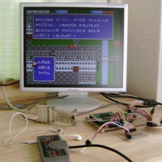
I think the hardware is working about 80% accurate now. Although I thought it would have been easy to implement everything in XC3S200, it now uses about 88% of the chip with area-optimized. But since this includes pretty much everything, so the rest is to fix bugs and accuracy should increase. Fixing the parts that don't work correctly or at all is rather matter of time than technical skill, so I just won't try too hard anymore on fixing incompatibilities.
The R-2R DAC used in the prototype 1 has some noticeable "vertical line" type of noise on the screen on the timing when PPU and CPU processing takes place. This is especially noticeable when the screen displays light clors. I can't distinguish whether this is due to the bad circuit quality by my hand wiring or this is to happen in the first place. I will insert a buffer to see if it gets any better.
As for the PCE controller, it didn't work with Vcc=3.3V. It was unclear what the root cause was, but it seemed that the pull-up resistors were unable to pull the level to 'H'. So I fed Vcc=5V to the controller, changed the controller output levels to 3.3V by 74VHC244, changed level of FPGA output to 5V by a TTL IC (74LSxxx), and it worked.
Since the PCE controllers have turbo features for button I and II, these can be used if you access the controller properly. The pin assignment of the MINI-DIN 8pin connector is as follows (the 'v' is the top hollow of the connector).
     v
   6 7 8
  3 4   5
   1  2

 1 --- Vcc           SEL=0:         SEL=1:
 2 --- D0            D0 = I         D0 = UP
 3 --- D1            D1 = II        D1 = RIGHT
 4 --- D2            D2 = SEL       D2 = DOWN
 5 --- D3            D3 = RUN       D3 = LEFT
 6 --- SEL
 7 --- CLR
 8 --- GND
State of 4 buttons can be read by changing SEL bit.
But the turbo doesn't work by only changing the SEL bit.
To use turbo, CLR needs to be used. The proper way seems to be:
Although I was a bit worried about screen aspect ratio, it turned out to be fairly close to the real hardware. I think the aspect ratio (probably) doesn't change because VGA's horizontal frequency is just twice the NTSC's.
I think I should start building prototype 2. The plan is to run both FC and PCE on it.
Added buffers before the R-2R ladder resistors. This was very effective that all the vertical lines (noise) are gone now. I also made a R-2R DAC NOTE. One major drawback of the R-2R DAC is that it needs so many parts (i.e. takes more space). Since there was not much to add, I took some pictures of the DAC boards.
A friend in Germany kindly donated me a Minimig V1.1 board. :-)
This FPGA board is originally designed for building a clone of the Amiga 500. Since the board has got a XC3S400, VGA(RGB444), 2x512x16bits SRAMs and PWM stereo audio output (2x1bit), it can also run my FC core.
So here it is.

While the prototype 1 used a DRAM for the CPU memory, Minimig only has SRAMs. So the part handling DRAM needs to be modified. Also, because the SRAMs on Minimig are connected to the same bus, FC core on this platform can't simultaneously access CPU memory and PPU memory. So the accesses to the CPU and PPU memories need to be multiplexed.
Due to Amiga supporting PAL video output, the PAL sub-carrier frequency of 4.433619[MHz] is generated as the master frequency on the Minimig board. FC, on the other hand, uses 21.47727[MHz] as its master frequency, so 4.433619*29/6 ~= 21.4291585[MHz] is generated using the DCM. Error is approx. 0.22[%]. The error should be small enough that you won't notice any difference. But the problem is that the minimum output frequency of the DCM seems to be 24[MHz]. Therefore 21.4291585[MHz] is out of the range. However it's working, so I just assume it's OK for now.
As for the audio, I have to use PWM. The output is 10 bits, so the sample rate is 21.4291585/(2^10) ~= 21[kHz]. I listened to the audio output, and indeed it sounded like so - pretty rough. Doubling the sample rate should be alot nicer and probably good enough. Simply doubling the DCM output frequency would resolve the above mentioned minimum frequency violation and the audio quality problems at the same time, but this in return violates the FC core's maximum operating frequency. Hmm...
The video output was changed from RGB555 to RGB444. This made bright colors rather look like white, and so made the contrast of the whole screen very high. It seems that FC needs at least RGB555 for proper color quality.
As you can see from the above photo, Minimig is designed to read data from MMC. After power-on, MMC + PIC MCU do the FPGA configuration. After that, the MMC + PIC MCU work as a floppy disk emulator in the original Amiga 500 design.
The FPGA configuration is done by the PIC MCU by reading "minimig1.bin" from MMC. This file is supposedly the Amiga 500 core, but actually this time it's the synthesized FC core.
The boot sequence after the FPGA configuration goes exactly the same as the prototype 1. Currently ROM images are still loaded via the RS232C port, as I haven't made the part which communicates with the PIC MCU.
Prototype 2 started to work. This platform is intended to run as many designs as possible (including the PCE). I ported my DIY FC as an example of system designs.
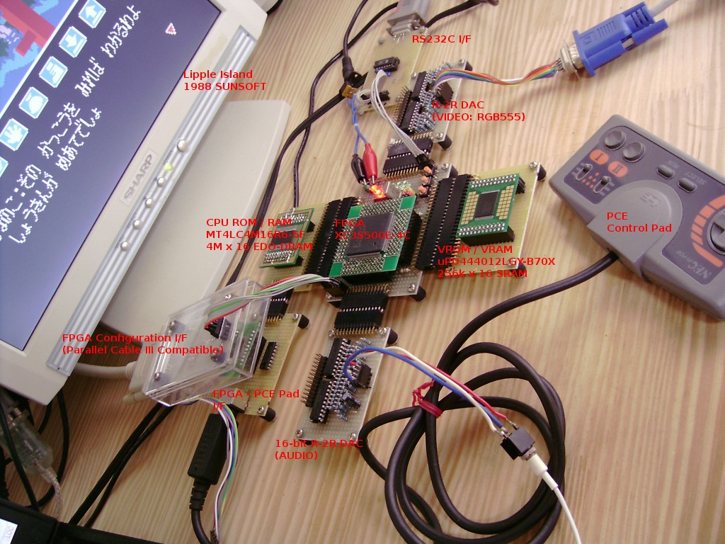
All major parts can be connected / disconnected. It is possible to build multiple FPGA modules and daisy-chain them.
The R-2R DACs are diverted from prototype 1 by adding a connector on one side of the boards. But there is a problem that R-2R DACs use too many I/O pins.
The audio output is currently 16-bit monaural and it already uses 16 I/O pins. If I make it stereo, then I would need 32 I/O pins and would run out of free I/O pins. So I need to start thinking of reducing number of I/O pins by either using an audio DAC with serial data input, or using PWM output.
As far as I have tested the PWM output on Minimig v1.1, I wasn't fully satisfied with its quality. So I'm thinking about using an audio DAC chip. However I already see some problems:
From availability of audio DAC ICs I would probably use:
As for FC implementation, I only have added some features of memory mapping ICs and haven't improved the main parts (as exact timings are still unclear). I works more or less OK, but still far from the level of perfection.
As I noticed by running my FC on prototype 2, the APU may have a minor bug which I haven't been able to notice. The DPCM (sound DMA) is not implemented yet. The Sprite DMA and DPCM DMA probably share some parts of the circuits.
The reason DQ3 and DQ4 still don't work can be found by comparing values of the program counter between FPGA and an emulator, but I haven't done it since it's not fun to do. ;) I would rather be interested in finding the following things:
An audio DAC using the uPD6376 worked.
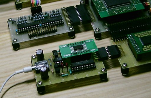
This is the DAC circuitry.
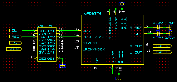
The level of uPD6376's input is 5[V] CMOS, while the output level of the FPGA is 3.3[V] CMOS. A 74LS244 is used to convert the FPGA's output level (3.3[V]) to 5[V]. A 74HCT244 can also be used, provided that its unused pins (11,13,15,17,19) are tied to either Vdd or GND.
Buffer amplifiers are added to the outputs of the DAC since the DAC did not seem capable of providing enough output current to drive earphones directly.

It wasn't as easy as I expected to design this simple circuitry. Since the power supply is single 5[V], I decided to use LM358N which should fully work in this condition. Since decoupling capacitor between the DAC's output and the OP-AMP's input is omitted, I had to test the circuitry and make sure the OP-AMP is able to output 0.6[V] when its input is 0.6[V] (i.e. the DAC's minimum output level). As a result, it works very well without noticeable noise at all, even though I did not use separate Vcc/GND for the analog part.
The center of the DAC's output level is 1.6[V]. This DAC IC expects signed 16-bit data as its input. -32768 is 0.6[V], 0 is 1.6[V] and 32767 is 2.6[V].
The OP-AMP works as a voltage follower. It has fairly high cut-off frequency that you can't notice whether or not the low-pass filter is working around the expected frequency by just listening.
I wanted the output transistors 2SC1815 and 2SA1015 to work as push-pull emitter follower, but it wasn't possible due to not enough power supply voltage to create the bias voltage. I think it is possible if the DAC and the OP-AMP were AC-coupled instead of DC-coupled and set the center voltage to 2.5[V], but I rather stuck to DC-coupling between them to have less capacitors through the audio signal path for better sound quality.
With these output transistors, it should be able to give "class A" drive to 32[Ohm] earphones. When 16[Ohm] earphones(headphones) are used, then the bottom 2SC1815 will cutoff above around 50% of the output, therefore it becomes "class AB" drive above that level (not tested).
The reason I did not simply use only transistors and used OP-AMP in addition to them is that the output had noticeable noise without the OP-AMP, and I could not stand with it. My guess is that the noise probably comes from the power supply and OP-AMP cancels it.
I built the following circuitry to try to confirm that the differential amplifier inside the OP-AMP has a certain value of CMRR (Common Mode Rejection Ratio) and that cancels noise from the power supply. This circuitry has two levels of differential amplifiers followed by an emitter follower. But this circuitry also had almost the same kind of noise I heard with the circuitry without the OP-AMP, so I'm kind of got lost here...
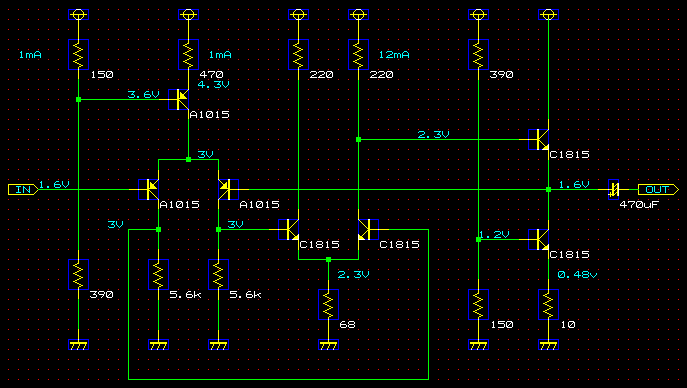
The values in the above circuit diagram are incorrect and does not match the actual values.
After all I'm not sure why my circuitry doesn't cancel the noise, but at least it seems the OP-AMP does it all for me...
Here is a sample verilog code to control uPD6376 by FPGA. It has 10-bit audio input (which is unusual and should be fixed for any use other than FC) since I just took it directly out from my FC.v. The expected clock frequency is 21.47727[MHz]. The uPD6376 can't operate above 10[MHz], so my FC divides the master clock by 4 and feeds the DAC ~5[MHz]. The playback sample rate is 21.47727/4/21 ~= 256[KHz], where value 21 (number of states) is explained below.
The total number of states in one sample transmission cycle is 21. 0-15 are data transmission states, and 16-20 are wait states for the DAC to actually output the transmitted data.
While control signals for uPD6376 is almost the same as shown in the datasheet, the part where it prepares output data should be modified. The output sample is calculated as an average of i_Audio in the 21-state period. In the case of FC, the audio output is only 10 bits, so value of i_Audio is simply added on evey state. Suppose maximum values are kept throughout the 21-state period, the accumulated value becomes 1023*21 = 21483, which is not too bad for a 16-bit audio output (doubling this value also works, but it resuled in the output volume too large for my earphones). So the "division" to get true average value is omitted.
If i_Audio is unsigned 16 bits, the maximum "average" value would be 65535 * 21 = 1376235 and this is a 21-bit value. So you should have r_DacSmaple[20:0], and modify the r_DacLatch assignment like below:
// note: only if r_DacSample is "unsigned"
r_DacLatch <= { ~r_DacSample[20], r_DacSample[19:5] };
The uPD6376 only accepts signed data, so the MSB needs to be inverted
to convert unsigned value (0-65535) to signed (-32768-32767).
When uPD6376 is powered, it outputs near-maximum value (~=2.6[V]). This results in the chip to output a large pop noise when it is powered. I think there are two major factors which make this DAC "cheep" (two for 500-yen at Akizuki electronic parts shop):
I noticed that uPD6376 is the previous version of uPD6379, which is used in Roland SC-55ST. The uPD6379's center voltage is 2.0[V], which seems slightly advanced to me. But the value upon power-on still seems to be a major problem that it says "it is recommended that you put mute circuitry after the output of the DAC" in the datasheet.
It now boots from SD/MMC. It finally works independently of PC and has become a stand-alone game cosole.
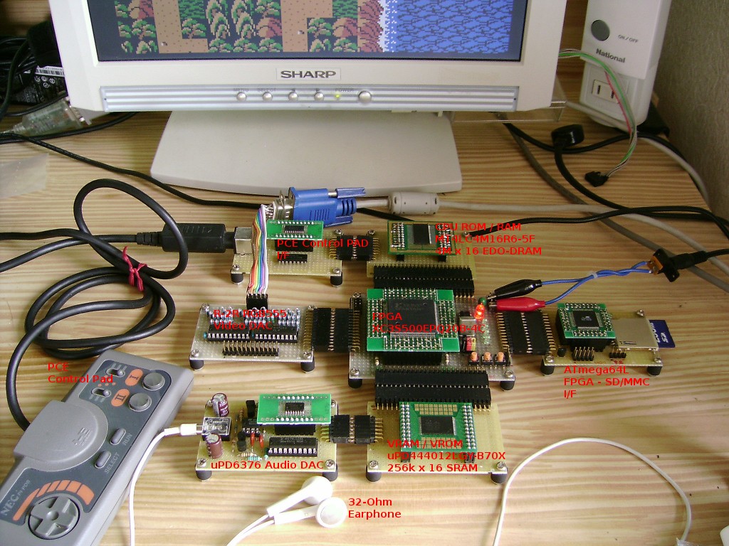
An ATMEL ATmega64L is used for the MCU. Unlike the PIC, the gcc supports the AVR chips very well. It is great that the start-up code is automatically generated by gcc and so we can start the actual development from the main() function.
The ATmega64L configures the FPGA and interfaces SD/MMC with the configured FPGA. After the cofiguration, the CPU of the FC accesses to the port only available in the boot period to communicate with the MCU.
The communication was initiall done byte-by-byte with handshaking, but it was not very efficient (around 20kB/s). So later I added a 8-byte FIFO. This in turn gave me a bug which took me pretty long to fix, but this dramatically increased transfer speed (close to 100kB/s). I think the speed is OK and so I decided not to use faster clock frequency only in the boot period, etc.
The FC's boot sequence is briefly as follows:
Steps 1-3 are done by the bootstrap, and 4 and later are done by the loader. The reason for separating the code into two parts is that I wanted the minimum bytes of ROM which is occupied by the FPGA. I think 256-byte ROM is enough to write a bootstrap code, and small enough to save FPGA area. The loader can be larger than the bootstrap, since it is loaded from the MCU (i.e. MMC). But since the current loader runs out of FC's RAM which is only 2kB, it also has size limitation of about 1.5kB, omitting 512 bytes for zero page and stack page. Currently the loader is about 1.2kB and is able to do the above steps 4-9.
Going a bit off-topic, but it surprizes me that Nindendo competed against the other game consoles with the FC which had only 2048 bytes of RAM, until they finally start selling the SFC. For example, PCE had 8192 bytes of RAM, and MD had 65536 bytes (32 times the FC!). Taking these facts into accout, I think Nintendo did an amazing job with the FC hardware.
Another digression, but I think the color palette of the
FC hardware should be estimated as one of the highest. Unlike the other
game consoles, the colors in the FC palette are actually chosen by the
game developer (Miyamoto) for game screen usage, instead of automatically
defining them by increasing/decreasing constant step of color value.
Therefore the hardware had good expression of light colors, and was able
to output rather warm colors. I think this helped the hardware to compete
against the other game consoles with much better performance.
Material movie on YouTube: "Shin Denshi-Rikkoku Nihon no Jijoden"
--> The official number of the total colors defined in the color palette was 52.
The design of the FC's control pad which first took this form and is followed by
almost all game consoles should also be estimated as one of the highest.
Well, as for my FC, the main parts haven't been improved for a long time, but I guess it is improving as a whole game console.
The boot sequence from SD/MMC can be used in PCE without much effort. PCE has a CPU which runs at 7.16[MHz], so I look forward to seeing some improvement in data transfer speed. --> 2009.05.05: Actually it worked. but data transfer wasn't as fast as I expected. I guess the bottleneck is in the MCU side.